| CPC H01L 25/18 (2013.01) [G11C 5/02 (2013.01); H01L 23/3142 (2013.01); H01L 23/49822 (2013.01); H01L 23/49838 (2013.01); H01L 23/5286 (2013.01); H01L 23/552 (2013.01); H01L 23/562 (2013.01); H01L 25/0655 (2013.01); H01L 25/50 (2013.01); H05K 1/0225 (2013.01); H05K 1/0271 (2013.01); H05K 1/0298 (2013.01); H05K 1/181 (2013.01); H05K 3/305 (2013.01); H10B 69/00 (2023.02); H01L 23/3121 (2013.01); H01L 2924/0002 (2013.01); H05K 2201/09136 (2013.01); H05K 2201/09681 (2013.01); H05K 2201/10159 (2013.01); Y02P 70/50 (2015.11)] | 11 Claims |
|
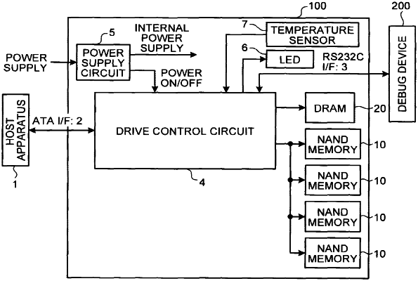
1. A semiconductor device comprising:
a substrate; and
a plurality of nonvolatile semiconductor memories on the substrate,
wherein the substrate includes:
a first metal layer having a first pattern density, the first metal layer being electrically connected to the nonvolatile semiconductor memories and being located on a first side of the substrate;
a second metal layer having a second pattern density, the second metal layer being located on a second side of the substrate;
a plurality of third metal layers disposed between the first and second metal layers and having respective third pattern densities; and
insulating layers provided between the first metal layer and a first one of the third metal layers adjacent to the first metal layer, between the second metal layer and a second one of the third metal layers adjacent to the second metal layer, and between adjacent ones of the third metal layers, wherein
a first group of metal layers includes n metal layers including the first metal layer and (n−1) adjacent third metal layers, a second group of n metal layers includes the second metal layer and (n−1) adjacent third metal layers different from the (n−1) third metal layers in the first group, a first density obtained from the first and third pattern densities of the first group of metal layers is substantially equal to a second density obtained from the second and third pattern densities of the second group of metal layers, and
at least one of the first and third pattern densities of the first group of metal layers and the second and third pattern densities of the second group of metal layers is 80% or greater.
|