| CPC H01L 25/18 (2013.01) [G11C 16/0483 (2013.01); G11C 16/08 (2013.01); G11C 16/26 (2013.01); H01L 24/08 (2013.01); H01L 25/0657 (2013.01); H01L 2224/08145 (2013.01); H01L 2924/1431 (2013.01); H01L 2924/14511 (2013.01)] | 20 Claims |
|
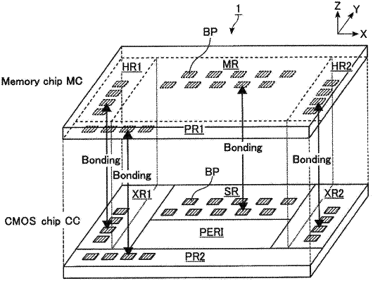
1. A semiconductor memory device comprising:
a substrate;
a first memory cell provided above the substrate;
a first bit line extending in a first direction, the first bit line being coupled to the first memory cell;
a first word line extending in a second direction intersecting the first direction, the first word line being coupled to the first memory cell;
a first transistor provided on the substrate, the first transistor being coupled to the first bit line; and
a second transistor provided below the first memory cell and on the substrate, the second transistor being coupled to the first word line.
|