| CPC H01L 25/0657 (2013.01) [H01L 21/30625 (2013.01); H01L 21/4853 (2013.01); H01L 21/563 (2013.01); H01L 21/78 (2013.01); H01L 25/50 (2013.01); H01L 2225/0651 (2013.01); H01L 2225/06506 (2013.01); H01L 2225/06517 (2013.01); H01L 2225/06562 (2013.01); H01L 2225/06575 (2013.01); H01L 2225/06582 (2013.01)] | 15 Claims |
|
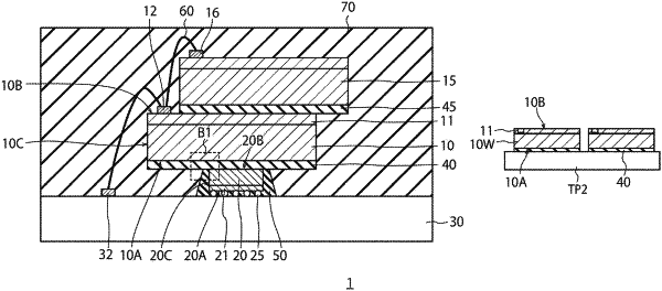
1. A method for manufacturing a semiconductor device, the method comprising:
providing a first semiconductor substrate having a first surface and a second surface opposite to each other;
forming a first resin layer on the first surface;
dicing the first semiconductor substrate into a plurality of first semiconductor chips;
providing a second semiconductor substrate having a third surface and a fourth surface opposite to each other;
coupling a connection bump on the third surface to a second resin layer;
connecting the connection bump to a wiring substrate; and
covering the connection bump between a second semiconductor chip and the wiring substrate with the second resin layer, wherein the second resin layer is disposed at a lower portion of a side surface of the second semiconductor chip.
|
|
12. A method for manufacturing a semiconductor device, the method comprising:
providing a first semiconductor substrate having a first surface and a second surface opposite to each other;
forming a first resin layer on the first surface;
dicing the first semiconductor substrate into a plurality of first semiconductor chips;
providing a second semiconductor substrate having a third surface and a fourth surface opposite to each other;
coupling a spacer chip to the first resin layer;
coupling a connection bump on the third surface to a second resin layer;
connecting the connection bump to a wiring substrate; and
covering the connection bump between a second semiconductor chip and the wiring substrate with the second resin layer, wherein the second resin layer is disposed at a lower portion of a side surface of the second semiconductor chip.
|