| CPC H01L 25/0657 (2013.01) [H01L 23/49816 (2013.01); H01L 25/50 (2013.01); H01L 2225/06517 (2013.01); H01L 2225/06548 (2013.01); H01L 2225/06562 (2013.01)] | 18 Claims |
|
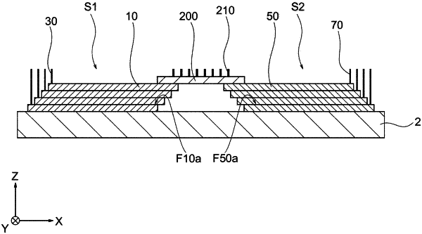
1. A semiconductor device, comprising:
a first stacked body including a plurality of first semiconductor chips stacked on top of one another in a first direction and offset relative to each other in a second direction perpendicular to the first direction;
a first columnar electrode coupled to an electrode pad of the first semiconductor chip and extending in the first direction;
a second stacked body arranged relative to the first stacked body in the second direction and including a plurality of second semiconductor chips stacked on top of one another in the first direction and offset relative to each other in the second direction;
a second columnar electrode coupled to an electrode pad of the second semiconductor chip and extending in the first direction; and
a third semiconductor chip arranged substantially equally spaced to the first columnar electrode and the second columnar electrode.
|