| CPC H01L 25/0657 (2013.01) [G11C 11/4096 (2013.01); H01L 24/07 (2013.01); H01L 24/16 (2013.01); H01L 24/48 (2013.01); H01L 25/50 (2013.01); H01L 25/18 (2013.01); H01L 2224/0233 (2013.01); H01L 2224/02373 (2013.01); H01L 2224/02375 (2013.01); H01L 2224/02381 (2013.01); H01L 2224/16225 (2013.01); H01L 2224/48145 (2013.01); H01L 2224/48225 (2013.01); H01L 2225/0651 (2013.01); H01L 2225/06506 (2013.01); H01L 2225/06517 (2013.01); H01L 2225/06527 (2013.01); H01L 2225/06558 (2013.01); H01L 2225/06562 (2013.01); H01L 2225/06565 (2013.01)] | 18 Claims |
|
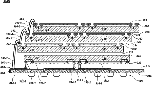
1. A method, comprising:
receiving read or write signals at a first memory die of a stacked die package from a substrate of the stacked die package, wherein an active surface of the first memory die faces an upper surface of the substrate; and
transmitting the read or write signals from the first memory die to an interconnect on the upper surface of the substrate via at least one direct chip attachment feature between the interconnect and the active surface of the first memory die; and
transmitting the read or write signals from the interconnect to a second memory die of the stacked die package via at least one wire bond between an active surface of the second memory die and the interconnect, wherein the second memory die is located over the first memory die.
|