| CPC H01L 25/0657 (2013.01) [G11C 13/004 (2013.01); G11C 13/0069 (2013.01); G11C 29/702 (2013.01); G11C 13/003 (2013.01); G11C 13/0026 (2013.01); G11C 13/0028 (2013.01); G11C 2013/0045 (2013.01); H01L 2225/06544 (2013.01); H10B 63/84 (2023.02)] | 19 Claims |
|
1. A device, comprising:
a first die comprising a first circuit, wherein the first circuit is configured to couple to a first buffer circuit and a second buffer circuit, and wherein the first buffer circuit is configured to receive first data generated by a first data source and the second buffer circuit is configured to receive second data generated by a second data source, and wherein the second data is independent of the first data;
a second die comprising a second circuit;
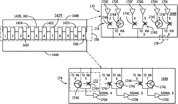
a material layer disposed between the first die and the second die and comprising a plurality of through-silicon vias (TSVs) for electrically coupling the first die to the second die, wherein a first TSV of the plurality of TSVs is associated with only three buffer circuits and is configured to electrically couple the first circuit to the second circuit, and a second TSV of the plurality of TSVs comprises a redundant TSV configured to electrically bypass the first TSV to couple the first circuit to the second circuit if a fault is detected in the first TSV; and
a control system configured to:
at a first time:
transmit the first data from the first circuit to the second circuit using the first TSV; and
transmit the second data from the first circuit to the second circuit using a third TSV of the plurality of TSVs; and
at a second time:
turn off a first switch and turn on a second switch to route third data from the first circuit to the second circuit using the third TSV, thereby bypassing the first TSV; and
turn off a third switch and turn on a fourth switch to route fourth data from the first circuit to the second circuit using the second TSV as opposed to the third TSV.
|