| CPC H01L 24/80 (2013.01) [H01L 24/74 (2013.01); H01L 2224/80121 (2013.01); H01L 2224/80894 (2013.01)] | 13 Claims |
|
8. A bonding facility comprising:
a loading part on which a container for accommodating a substrate is seated;
a substrate conveying part configured to convey the substrate from the container seated on the loading part;
a bonding part configured to bond a chip to the substrate provided from the substrate conveying part; and
an inspection part configured to receive, from the substrate conveying part, the substrate processed by the bonding part and inspect the chip bonded to the substrate,
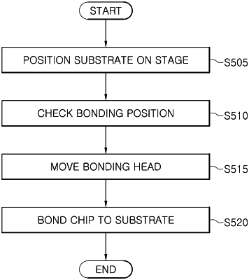
wherein the bonding part comprises:
a stage on which the substrate is seated;
a gantry installed above the stage;
a bonding unit configured to bond the chip to the substrate while moving along the gantry; and
a control part configured to move the bonding unit to align the bonding unit with a bonding position on the substrate, the control part being configured to control the bonding unit to allow the bonding unit to bond the chip at the bonding position of the substrate, and
wherein the control part determines a movement distance of the bonding unit based on a weighted sum of a number of continuous operations and an idle time of the bonding unit.
|