| CPC H01L 24/75 (2013.01) [H01L 21/4853 (2013.01); H01L 21/563 (2013.01); H01L 24/27 (2013.01); H01L 24/32 (2013.01); H01L 24/73 (2013.01); H01L 24/81 (2013.01); H01L 24/83 (2013.01); H01L 24/92 (2013.01); H01L 24/13 (2013.01); H01L 24/16 (2013.01); H01L 24/94 (2013.01); H01L 2224/131 (2013.01); H01L 2224/13111 (2013.01); H01L 2224/13147 (2013.01); H01L 2224/16227 (2013.01); H01L 2224/27003 (2013.01); H01L 2224/2783 (2013.01); H01L 2224/2784 (2013.01); H01L 2224/27436 (2013.01); H01L 2224/32013 (2013.01); H01L 2224/32058 (2013.01); H01L 2224/32059 (2013.01); H01L 2224/32105 (2013.01); H01L 2224/32106 (2013.01); H01L 2224/32225 (2013.01); H01L 2224/73103 (2013.01); H01L 2224/73204 (2013.01); H01L 2224/7532 (2013.01); H01L 2224/75251 (2013.01); H01L 2224/75252 (2013.01); H01L 2224/75303 (2013.01); H01L 2224/75312 (2013.01); H01L 2224/75318 (2013.01); H01L 2224/75745 (2013.01); H01L 2224/8182 (2013.01); H01L 2224/81169 (2013.01); H01L 2224/81191 (2013.01); H01L 2224/81193 (2013.01); H01L 2224/81203 (2013.01); H01L 2224/81815 (2013.01); H01L 2224/81895 (2013.01); H01L 2224/83203 (2013.01); H01L 2224/83862 (2013.01); H01L 2224/9211 (2013.01); H01L 2224/9212 (2013.01); H01L 2224/94 (2013.01)] | 18 Claims |
|
1. A thermocompression-bonding apparatus, comprising:
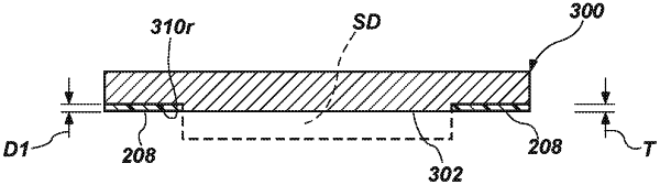
a bond tip, the thermocompression-bonding apparatus configured to apply heat and pressure to a semiconductor directly by a bottom surface of the bond tip, the bottom surface comprising:
a planar die-contact area, a length and a width of the planar die-contact area substantially corresponding to a length and a width of a semiconductor die to be received on the planar die-contact area;
a planar peripheral portion surrounding the planar die-contact area, the planar peripheral portion oriented parallel to the planar die-contact area; and
a low-surface-energy material secured to the planar peripheral portion of the bottom surface, wherein the low-surface-energy material is absent from the planar die-contact area.
|