| CPC H01L 24/14 (2013.01) [H01L 21/50 (2013.01); H01L 23/5385 (2013.01); H01L 23/5386 (2013.01); H01L 24/95 (2013.01); H01L 29/7393 (2013.01); H01L 2021/60022 (2013.01)] | 13 Claims |
|
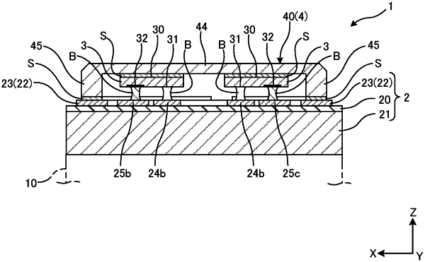
1. A semiconductor module, comprising:
a laminated substrate including an insulating plate, a circuit pattern arranged on an upper surface of the insulating plate, and a heat dissipating plate arranged on a lower surface of the insulating plate opposite to the upper surface of the insulating plate; and
a semiconductor device having an upper surface and a lower surface opposite to the upper surface and facing the circuit pattern, the semiconductor device including a collector electrode arranged on the upper surface thereof, and an emitter electrode and a gate electrode arranged on the lower surface thereof, the emitter electrode being positioned closer to a periphery of the laminated substrate than is the gate electrode in a plan view of the semiconductor module; and
bumps respectively bonding the emitter electrode and the gate electrode to an upper surface of the circuit pattern, wherein
each of the bumps consists of a sintered material containing metal particles and is constricted in a middle portion thereof in a thickness direction orthogonal to a surface of the insulating plate.
|