| CPC H01L 24/14 (2013.01) [H01L 23/3114 (2013.01); H01L 23/3128 (2013.01); H01L 23/3735 (2013.01); H01L 23/53209 (2013.01)] | 17 Claims |
|
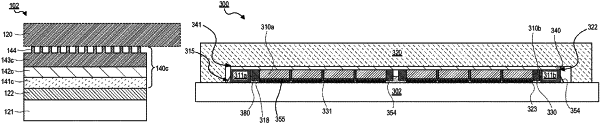
1. A semiconductor package, comprising:
a plurality of first dies on a substrate;
an interface layer over the plurality of first dies;
a backside metallization (BSM) layer directly on the interface layer, wherein the BSM layer includes a first conductive layer, a second conductive layer, and a third conductive layer; and
a heat spreader over the BSM layer, wherein the first conductive layer of the BSM layer is directly coupled to the interface layer, and wherein the third conductive layer of the BSM layer is directly coupled to the heat spreader.
|