| CPC H01L 23/66 (2013.01) [H01L 21/4853 (2013.01); H01L 21/4857 (2013.01); H01L 21/565 (2013.01); H01L 23/3121 (2013.01); H01L 23/5383 (2013.01); H01L 23/5386 (2013.01); H01L 23/5389 (2013.01); H01L 24/19 (2013.01); H01L 24/20 (2013.01); H01Q 1/38 (2013.01); H01L 2223/6622 (2013.01); H01L 2223/6677 (2013.01); H01L 2224/214 (2013.01)] | 20 Claims |
|
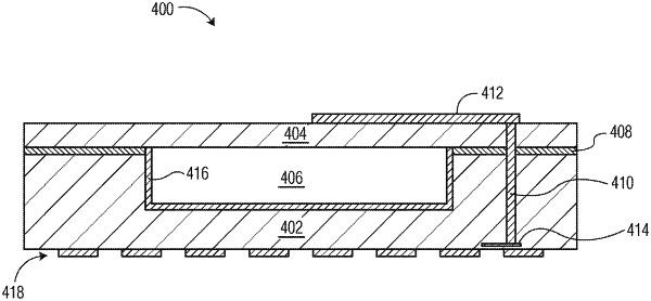
1. A semiconductor device comprising:
a base die having an active surface and a backside surface, an integrated circuit formed at the active surface;
a cap die having a top surface and a bottom surface, the bottom surface of the cap die bonded to the backside surface of the base die;
a metal trace formed over the top surface of the cap die;
a dielectric layer disposed between the metal trace and the top surface of the cap die;
a conductive via formed through the base die and the cap die, the conductive via interconnecting the metal trace and a conductive trace of the integrated circuit; and
a cavity formed under the metal trace, a portion of the cap die remaining between the metal trace and the cavity.
|