| CPC H01L 23/562 (2013.01) [H01L 21/76816 (2013.01); H01L 21/76877 (2013.01); H01L 23/5226 (2013.01); H01L 23/5283 (2013.01); H10B 41/27 (2023.02); H10B 43/27 (2023.02)] | 20 Claims |
|
1. An apparatus comprising:
a substrate;
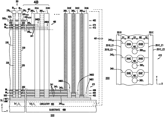
tiers located one over another over the substrate, the tiers including respective memory cells and control gates for the memory cells, the control gates including a control gate closest to the substrate than other control gates, the control gates including respective portions that collectively form a staircase structure;
conductive contacts contacting the control gates at a location of the staircase structure, the conductive contacts having different lengths extending vertically from the substrate, the conductive contacts including a conductive contact contacting the control gate;
a dielectric structure adjacent sidewalls of the control gates of the tiers; and
support structures adjacent the conductive contacts and electrically separated from the control gates and the conductive contacts, the support structures having lengths extending vertically from the substrate and extending through at least a portion of the control gates, the support structures including a support structure closest to the conductive contact than other support structures, the support structure located at a distance from an edge of the dielectric structure, wherein a ratio of a width of the support structure over the distance is ranging from 1.6 to 2.0.
|