| CPC H01L 23/528 (2013.01) [H01L 21/7682 (2013.01); H01L 23/5222 (2013.01); H01L 29/0649 (2013.01)] | 20 Claims |
|
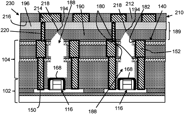
1. A method comprising:
forming an opening in a dielectric layer between adjacent conductors;
forming a dual dielectric layer over the dielectric layer, the dual dielectric layer including:
forming a first dielectric layer over the opening to fill a first portion of the opening, wherein a remainder of the opening is free of the first dielectric layer;
forming a second dielectric layer on a top surface of the first dielectric layer, leaving a remainder of the opening unfilled, wherein the second dielectric layer is devoid of wiring, and wherein the remainder of the opening below the second dielectric layer defines an air gap structure; and
forming a wiring layer above the air gap structure.
|