| CPC H01L 23/481 (2013.01) [H01L 23/315 (2013.01)] | 23 Claims |
|
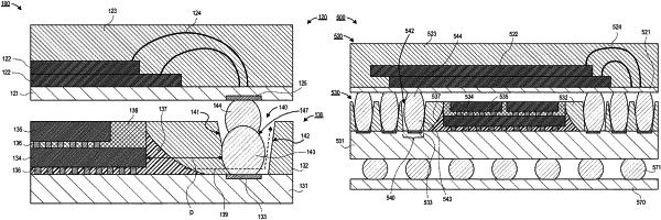
1. An electronic package, comprising:
a package substrate;
a first die electrically coupled to the package substrate;
a second die coupled to a top surface of the first die;
a mold layer over the package substrate and around the first die and the second die;
a through mold opening through the mold layer; and
a through mold interconnect (TMI) in the through mold opening, wherein a center of the TMI is offset from a center of the through mold opening, the TMI laterally spaced apart from the first die and laterally spaced apart from the second die.
|