| CPC H01L 23/13 (2013.01) [H01L 21/4857 (2013.01); H01L 21/565 (2013.01); H01L 23/3128 (2013.01); H01L 23/49816 (2013.01); H01L 23/49822 (2013.01); H01L 25/0657 (2013.01); H01L 25/18 (2013.01); H01L 25/50 (2013.01); H01L 21/4853 (2013.01); H01L 24/16 (2013.01); H01L 24/32 (2013.01); H01L 24/48 (2013.01); H01L 24/73 (2013.01); H01L 2224/16146 (2013.01); H01L 2224/16227 (2013.01); H01L 2224/32145 (2013.01); H01L 2224/48091 (2013.01); H01L 2224/48106 (2013.01); H01L 2224/48227 (2013.01); H01L 2224/73253 (2013.01); H01L 2224/73265 (2013.01); H01L 2225/0651 (2013.01); H01L 2225/06513 (2013.01); H01L 2225/06517 (2013.01); H01L 2225/06541 (2013.01); H01L 2225/06565 (2013.01); H01L 2225/06586 (2013.01); H01L 2924/1432 (2013.01); H01L 2924/1434 (2013.01)] | 7 Claims |
|
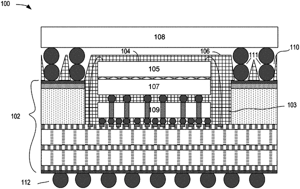
1. A method comprising:
forming a substrate with a cavity defining a lower surface and an upper surface parallel to the lower surface;
forming solder spheres on the upper surface;
attaching one or more die(s) to the lower surface of the substrate, wherein the one or more die(s) extend beyond the upper surface;
overmolding the one or more die(s) and the solder spheres; and
forming through mold vias to expose the solder spheres.
|