| CPC H01L 22/14 (2013.01) [C23C 16/52 (2013.01); G01R 31/2621 (2013.01); H01L 21/67253 (2013.01)] | 20 Claims |
|
1. A system for in-situ monitoring of semiconductor devices during chemical vapor deposition, comprising:
a reactor having a sealed chamber for carrying out chemical vapor deposition (CVD) on semiconductor devices, wherein the reactor is configured with a plurality of openings for passaging of reactive gases and for in-situ monitoring of the semiconductor devices within the sealed chamber during the CVD; and
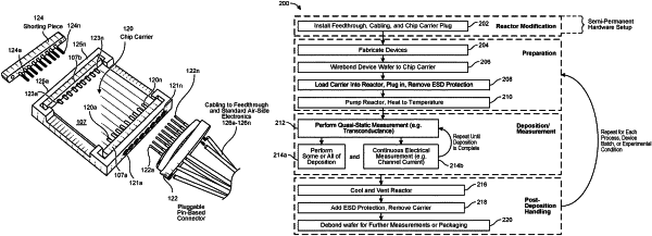
a chip carrier configured to be disposed within the sealed chamber, wherein the chip carrier is configured for mounting at least one partially fabricated semiconductor device on a base, wherein the chip carrier comprises a plurality of metallized bonding pads disposed along both peripheral edges on a same surface of the base for making electrical connections to one or more metallized pads or contacts on the at least one partially fabricated semiconductor device through bonding wires, such that each of the plurality of metallized bonding pads is individually and electrically connected to a respective port on the chip carrier for in-situ monitoring of electrical parameters of the at least one partially fabricated semiconductor device during the CVD, wherein electrical currents or electrical signals are exchanged between the at least one partially fabricated semiconductor device and a source-measure unit (SMU) disposed external to the sealed chamber through a connector and wire harness that is electrically coupled to a plurality of ports on one peripheral edge of the chip carrier within the sealed chamber,
wherein the SMU comprises a plurality of measurement equipment configured to perform in-situ measurements of the electrical parameters of the at least one partially fabricated semiconductor device during the CVD.
|