| CPC H01L 21/823425 (2013.01) [H01L 21/823412 (2013.01); H01L 21/823431 (2013.01); H01L 27/088 (2013.01); H01L 27/0886 (2013.01)] | 20 Claims |
|
15. A method, comprising:
forming a first semiconductor fin and a second semiconductor fin;
forming a sacrificial gate structure across the first and second semiconductor fins;
forming a sidewall spacer layer on sidewalls of the first and second semiconductor fins;
recess etching the first and second semiconductor fins exposed by the sacrificial gate structure;
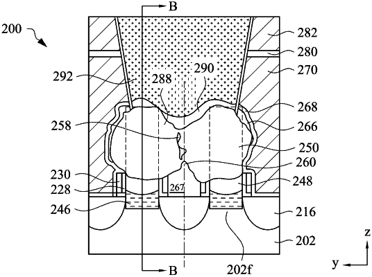
forming an epitaxial source/drain feature from the first and second fins, wherein the epitaxial source/drain feature includes a top surface, a bottom surface opposite the top surface, and a side surface connecting the top surface and bottom surface, a first void is formed between the top surface and the bottom surface;
depositing a CESL (contact etch stop layer) over the epitaxial source/drain feature;
forming an ILD (inter layer dielectric) layer over the CESL;
forming a contact opening through the ILD layer and the CESL layer to expose the epitaxial source/drain feature; and
forming a source/drain contact feature in the contact opening;
wherein each of the first and second semiconductor fin comprises two or more channel layers and two or more sacrificial semiconductor layers alternately arranged with the two more channel layers.
|