| CPC H01L 21/78 (2013.01) [H01L 23/50 (2013.01); H01L 24/94 (2013.01); H01L 31/02002 (2013.01); H01L 31/0216 (2013.01); H01L 31/186 (2013.01); H01L 33/0093 (2020.05); H01L 33/0095 (2013.01); H01L 33/44 (2013.01); H01L 33/62 (2013.01); H01L 24/32 (2013.01); H01L 24/83 (2013.01); H01L 2224/32225 (2013.01); H01L 2224/83192 (2013.01); H01L 2224/83801 (2013.01)] | 20 Claims |
|
1. A method of producing a semiconductor device comprising:
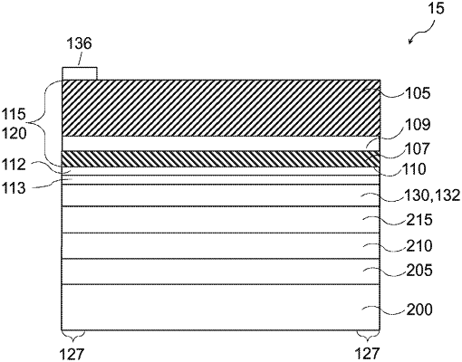
forming at least one semiconductor layer over a growth substrate to form a semiconductor body;
thereafter applying a first compressively stressed layer over the semiconductor body to form a workpiece;
wherein the first compressively stressed layer comprises a material selected from tantalum, molybdenum, niobium, compounds, or combinations thereof;
thereafter applying the workpiece to a carrier; so that the first compressively stressed layer is arranged between the semiconductor body and the carrier; and
separating the workpiece into individual semiconductor devices.
|