| CPC H01L 21/76877 (2013.01) [H01L 21/76802 (2013.01); H01L 23/5226 (2013.01); H01L 23/53214 (2013.01); H01L 23/53228 (2013.01); H10B 41/27 (2023.02); H10B 43/27 (2023.02)] | 6 Claims |
|
1. A microelectronic device, comprising:
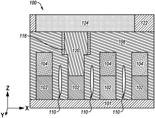
conductive bit lines extending in a first horizontal direction;
insulative line structures vertically adjacent the conductive bit lines and extending in the first horizontal direction;
partially filled trenches intervening between the conductive bit lines in a second horizontal direction orthogonal to the first horizontal direction, the partially filled trenches comprising:
an isolation material on side surfaces of the conductive bit lines and the insulative line structures; and
air gaps surrounded by the isolation material and vertically overlapping the conductive bit lines;
conductive contact structures vertically extending through portions of the insulative line structures and directly physically contacting the conductive bit lines, the conductive contact structures partially vertically overlapping the air gaps; and
conductive pad structures vertically adjacent the conductive contact structures;
wherein vertically lower portions of the conductive contact structures are relatively horizontally narrower than vertically upper portions of the conductive contact structures; and
further comprising dielectric spacer structures physically contacting side surfaces of the vertically upper portions of the conductive contact structures, but not physically contacting side surfaces of the vertically lower portions of the conductive contact structures.
|