| CPC H01L 21/76849 (2013.01) [H01L 21/7685 (2013.01); H01L 21/76814 (2013.01); H01L 21/76825 (2013.01); H01L 21/76826 (2013.01); H01L 21/76829 (2013.01); H01L 21/76831 (2013.01); H01L 21/76834 (2013.01); H01L 21/76865 (2013.01); H01L 21/76883 (2013.01); H01L 21/76897 (2013.01)] | 5 Claims |
|
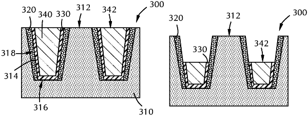
1. A processing method comprising:
providing a substrate comprising a dielectric material with at least one feature formed thereon, the at least one feature having at least one sidewall and a bottom, a distance from a surface of the dielectric material to the bottom of the feature defining a depth of the feature;
passivating the dielectric material at the sidewall of the feature to form a passivated dielectric layer, wherein passivating the dielectric material at the sidewall of the feature forms a gradient passivated dielectric layer so that a portion of the sidewall from surface of the dielectric material to a predetermined depth is modified so that removal of the barrier layer from the passivated dielectric material is easier than removal of the barrier layer from the dielectric material;
forming a barrier layer on the at least one sidewall on the passivated dielectric layer and the bottom of the at least one feature;
depositing a metal layer in the feature to fill the at least one feature; and
removing a portion of the metal layer and the barrier layer to a predetermined depth and remove the barrier layer from the passivated dielectric layer.
|