| CPC H01L 21/76224 (2013.01) [H01L 21/304 (2013.01); H01L 21/7624 (2013.01); H01L 27/1203 (2013.01); H10B 10/12 (2023.02)] | 16 Claims |

|
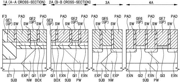
1. A method of manufacturing a semiconductor device, comprising steps of:
(a) providing an SOI substrate having a semiconductor substrate, an insulating layer formed on the semiconductor substrate, and a semiconductor layer formed on the insulating layer;
(b) after the (a), forming a first conductive film on the semiconductor layer;
(c) after the (b), forming a first insulating film on the first conductive film;
(d) after the (c), patterning the first conductive film and the first insulating film, thereby forming a gate pattern and a cap film;
(e) after the (d), implanting an impurity into the semiconductor layer located on both sides of the gate pattern, thereby forming a first impurity region;
(f) after the (e), forming a first sidewall spacer made of a second insulating film on a side surface of the gate pattern;
(g) after the (f), forming a second conductive film on the first impurity region so as to cover the gate pattern, the cap film, and the first sidewall spacer;
(h) after the (g), performing a polishing process to the second conductive film until the cap film is exposed;
(i) after the (h), patterning a part of the second conductive film, thereby forming a pad layer made of the remaining second conductive film;
(j) after the (i), filling a portion, from where the second conductive film has been removed, with a third insulating film; and
(k) after the (j), performing a polishing process to the cap film, the first sidewall spacer, the third insulating film, and the pad layer until the cap film is removed and the gate pattern is exposed.
|