| CPC H01L 21/6719 (2013.01) [G01N 21/73 (2013.01); H01J 49/105 (2013.01); H01L 21/6708 (2013.01); H01L 21/6715 (2013.01); H01L 21/67051 (2013.01); H01L 21/67126 (2013.01); H01L 21/67259 (2013.01); H01L 21/67748 (2013.01); H01L 21/67772 (2013.01); H01L 22/14 (2013.01); H01L 22/34 (2013.01); G01N 2033/0095 (2013.01); H01J 49/00 (2013.01); H01L 22/12 (2013.01)] | 17 Claims |
|
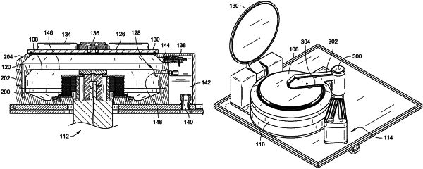
1. A chamber for decomposing and scanning a surface of a semiconducting wafer comprising:
a chamber body defining an interior region and a first aperture at a top portion of the chamber to receive a semiconducting wafer into the interior region of the chamber body;
a ledge projecting into the interior region at an intermediate portion of the chamber body between the top portion of the chamber body and a bottom portion of the chamber body, the ledge defining a second aperture within the interior region at the intermediate portion;
a wafer support configured to hold at least a portion of the semiconducting wafer, the wafer support positionable between at least a first position adjacent the first aperture and a second position adjacent the second aperture within the interior region of the chamber body;
a motor system operably coupled with the wafer support, the motor system configured to control a vertical position of the wafer support with respect to the chamber body at least to the first position for access to the semiconducting wafer by a scanning nozzle and the second position for decomposition of a surface of the semiconducting wafer;
a nebulizer positioned within an aperture in a wall of the chamber body and configured to spray a decomposition fluid into the interior region of the chamber body, the nebulizer extending no further than an inner periphery of the wall of the chamber body during spraying of the decomposition fluid;
a gas outlet port beneath the second aperture within the interior region of the chamber body; and
a controller coupled to a gas source, the controller configured to introduce gas from the gas source to the gas outlet port during introduction of the decomposition fluid onto the surface of the semiconducting wafer by the nebulizer at a pressure greater than a pressure of the decomposition fluid introduction when the wafer support is positioned at the second position.
|