| CPC H01L 21/4882 (2013.01) [C04B 37/021 (2013.01); H01L 23/3735 (2013.01); H05K 1/0203 (2013.01); H05K 1/0306 (2013.01); H05K 3/20 (2013.01); C04B 2237/343 (2013.01); C04B 2237/366 (2013.01); C04B 2237/368 (2013.01); C04B 2237/402 (2013.01); C04B 2237/704 (2013.01); C04B 2237/706 (2013.01)] | 7 Claims |
|
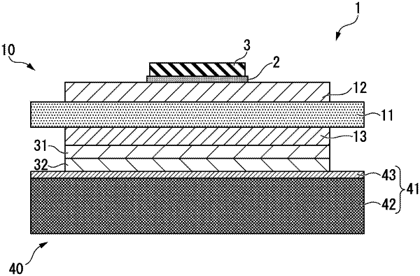
1. A method for producing an insulating circuit substrate with a heat sink including an insulating circuit substrate and a heat sink,
the insulating circuit substrate including a circuit layer that is formed on a first surface of an insulating layer and a metal layer that is formed on a second surface of the insulating layer,
the heat sink being bonded to the metal layer side of the insulating circuit substrate,
the metal layer being formed of aluminum having a purity of 99 mass % or higher,
an indentation hardness of the metal layer being lower than 50 mgf/μm2,
a bonding surface of the heat sink with the insulating circuit substrate being formed of aluminum or an aluminum alloy having a solidus temperature of 650° C. or lower, and
the method comprising:
a circuit layer and metal layer forming step of forming the circuit layer and the metal layer by laminating the circuit layer via a first brazing material on the first surface of the insulating layer, and laminating the metal layer via a second brazing material on the second surface of the insulating layer, in order to obtain the insulating circuit substrate;
an aluminum bonding layer forming step of forming an aluminum bonding layer formed of an aluminum alloy having a solidus temperature of 650° C. or lower on a surface of the metal layer opposite to the insulating layer; and
a heat sink bonding step of bonding the heat sink to the aluminum bonding layer by laminating a copper bonding material formed of copper or a copper alloy between the aluminum bonding layer and the bonding surface of the heat sink and bonding the aluminum bonding layer and the copper bonding material to each other and bonding the copper bonding material and the heat sink to each other by solid phase diffusion bonding.
|