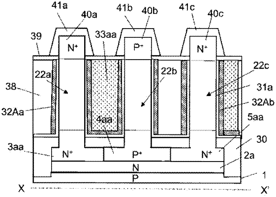
| CPC H01L 21/3085 (2013.01) [H01L 21/02587 (2013.01); H01L 29/1054 (2013.01); H01L 29/66666 (2013.01)] | 8 Claims |

|
1. A method for manufacturing a pillar-shaped semiconductor device, comprising the steps of:
forming a first mask material layer extending in a band shape in one direction in plan view on a semiconductor layer on a substrate;
etching the semiconductor layer using the first mask material layer as a mask to form a first band-shaped semiconductor pillar;
forming a first material layer so as to cover the first mask material layer, the first band-shaped semiconductor pillar, and a portion of the substrate around an outer periphery of the first band-shaped semiconductor pillar;
forming a second material layer so as to cover the first material layer;
planarizing the first material layer and the second material layer such that upper surfaces thereof are located at the same height as an upper surface of the first mask material layer;
etching a top portion of the first material layer using the first mask material layer and the second material layer as a mask to form first recesses;
forming a second mask material layer so as to fill the first recesses above the top portion of the first material layer and such that an upper surface of the second mask material layer is located at the same height as the upper surface of the first mask material layer;
removing the second material layer;
etching the first material layer using the first mask material layer and the second mask material layer as a mask to form a first band-shaped material pillar and a second band-shaped material pillar based on the first material layer on both sides of the first band-shaped semiconductor pillar in plan view;
forming a first semiconductor layer so as to cover the first mask material layer, the second mask material layer, the first band-shaped semiconductor pillar, the first band-shaped material pillar, the second band-shaped material pillar, and the substrate;
forming a third material layer so as to cover the first semiconductor layer;
planarizing the first semiconductor layer and the third material layer such that upper surfaces thereof are located at the same height as the upper surface of the first mask material layer;
etching a top portion of the first semiconductor layer using the first mask material layer, the second mask material layer, and the third material layer as a mask to form second recesses;
forming a third mask material layer so as to fill the second recesses above the top portion of the first semiconductor layer and such that an upper surface of the third mask material layer is located at the same height as the upper surface of the first mask material layer;
removing the third material layer;
etching the first semiconductor layer using the first mask material layer, the second mask material layer, and the third mask material layer as a mask to form a second band-shaped semiconductor pillar and a third band-shaped semiconductor pillar based on the first semiconductor layer outside the first band-shaped material pillar and the second band-shaped material pillar in plan view;
removing the first band-shaped material pillar and the second band-shaped material pillar;
forming a fourth material layer around outer peripheries of the first band-shaped semiconductor pillar, the second band-shaped semiconductor pillar, and the third band-shaped semiconductor pillar such that an upper surface of the fourth material layer is located at the same height as the upper surface of the first mask material layer;
forming a fourth mask material layer extending in a band shape on the first mask material layer, the third mask material layer, and the fourth material layer in a direction perpendicular to the direction in which the first mask material layer extends in a band shape in plan view; and
etching the first band-shaped semiconductor pillar, the second band-shaped semiconductor pillar, and the third band-shaped semiconductor pillar using the fourth mask material layer as a mask to form a first semiconductor pillar, a second semiconductor pillar, and a third semiconductor pillar,
wherein pillar-shaped semiconductor devices having channels in the first semiconductor pillar, the second semiconductor pillar, and the third semiconductor pillar are formed.
|