| CPC H01G 4/30 (2013.01) [H01G 4/0085 (2013.01); H01G 4/012 (2013.01); H01G 4/2325 (2013.01); C04B 35/48 (2013.01)] | 19 Claims |
|
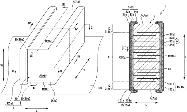
1. An electronic component comprising:
a multilayer body including dielectric layers and internal electrode layers laminated alternately on each other; and
external electrode layers on opposing end surfaces of the multilayer body in a length direction orthogonal or substantially orthogonal to a lamination direction; wherein
each of the external electrode layers is connected with the internal electrode layers;
the dielectric layers each include at least one of Ca, Zr, and Ti;
the internal electrode layers each include Cu; and
when a dimension in the lamination direction of the multilayer body is defined as TO, a dimension in the length direction of the multilayer body is defined as L0, and a dimension in a width direction orthogonal or substantially orthogonal to the lamination direction and the length direction is defined as W0, a relationship of L0<W0<T0 is satisfied.
|