| CPC G11C 16/14 (2013.01) [G11C 11/5635 (2013.01); G11C 16/0483 (2013.01); G11C 16/08 (2013.01); G11C 16/10 (2013.01); G11C 16/26 (2013.01); G11C 29/42 (2013.01); H10B 43/27 (2023.02); H10B 43/35 (2023.02); G11C 16/3445 (2013.01)] | 12 Claims |
|
1. A semiconductor memory device comprising:
a source line;
a bit line;
a memory cell array including a memory string electrically connected between the bit line and the source line, the memory string including a first select transistor, a second select transistor, and a plurality of memory cell transistors electrically connected in series between the first select transistor and the second select transistor, the memory cell transistors including
a first memory cell transistor,
a second memory cell transistor, wherein the first memory cell transistor is between the first select transistor and the second memory cell transistor,
a third memory cell transistor, and
a fourth memory cell transistor, wherein the fourth memory cell transistor is between the third memory cell transistor and the second select transistor;
a plurality of word lines electrically connected to gates of the memory cell transistors, respectively, the word lines including
a first word line electrically connected to the gate of the first memory cell transistor,
a second word line electrically connected to the gate of the second memory cell transistor,
a third word line electrically connected to the gate of the third memory cell transistor, and
a fourth word line electrically connected to the gate of the fourth memory cell transistor;
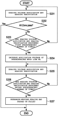
a sequencer configured to perform an erase operation on the memory cell transistors, the erase operation including an erase voltage apply operation and an erase verify operation, the erase voltage apply operation using a Gate-Induced-Drain-Leakage (GIDL) current,
wherein
during the erase operation,
at a first timing,
a first voltage is applied to the first word line, and
a second voltage is applied to the second word line,
a third voltage is applied to the third word line, and
a fourth voltage is applied to the fourth word line, and
at a second timing after the first timing
a fifth voltage is applied to the first word line, the fifth voltage being higher than the first voltage, and
a sixth voltage is applied to the fourth word line, the sixth voltage being higher than the fourth voltage.
|