| CPC G11C 13/0069 (2013.01) [G11C 13/003 (2013.01); G11C 13/004 (2013.01); G11C 13/0061 (2013.01); G11C 2013/0078 (2013.01)] | 20 Claims |
|
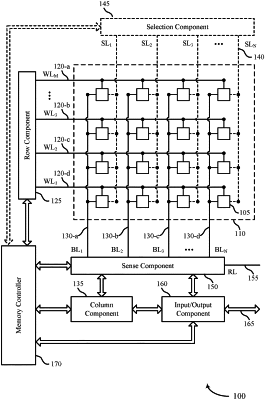
1. A method, comprising:
receiving a write command indicating a set of data to be written to a plurality of memory cells; and
performing a write operation based at least in part on the write command, wherein performing the write operation comprises applying a first write signal to a first set of memory cells of the plurality of memory cells that are to be switched from a first logic state to a second logic state as a result of the write command and have a characteristic that does not satisfy a threshold, and applying a second write signal to a second set of memory cells of the plurality of memory cells that are to be switched from the first logic state to the second logic state as a result of the write command and have the characteristic satisfying the threshold.
|