| CPC G11C 11/5642 (2013.01) [G11C 11/5628 (2013.01); G11C 16/10 (2013.01); G11C 16/26 (2013.01); G11C 16/30 (2013.01)] | 20 Claims |
|
1. A method comprising:
receiving, by a processing device, a request to read data from a memory cell of a memory device coupled with the processing device;
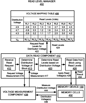
determining a voltage distribution parameter value associated with the memory cell of the memory device;
determining a set of read levels associated with the voltage distribution parameter value, wherein each read level in the determined set of read levels corresponds to a respective voltage distribution of the memory cell, wherein determining the set of read levels associated with the voltage distribution parameter value comprises:
responsive to determining that a voltage mapping table does not include the voltage distribution parameter value, determining the set of read levels using interpolation based on first and second parameter values that are included in the voltage mapping table, wherein the set of read levels is determined as an average of a first set of read levels that correspond to the first parameter value and a second set of read levels that correspond to the second parameter value; and
reading, using the determined set of read levels, data from the memory cell of the memory device.
|