| CPC G11C 11/5642 (2013.01) [G11C 11/5671 (2013.01); G11C 16/0483 (2013.01); G11C 16/26 (2013.01)] | 20 Claims |
|
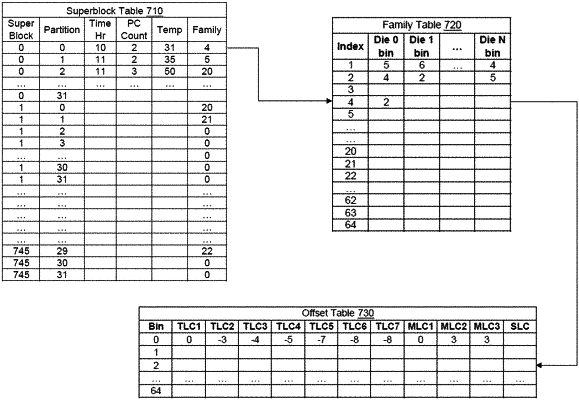
1. A method comprising:
creating a block family associated with a memory device;
associating the block family with a threshold voltage offset bin;
determining a set of read level voltage offsets such that, when applied to a base read level threshold voltage associated with the block family, result in a suboptimal error rate not exceeding a maximum allowable error rate, wherein the suboptimal error rate exceeds a minimum error rate for the block family; and
associating the set of read level voltage offsets with the threshold voltage offset bin.
|