| CPC G11C 11/4093 (2013.01) [H10B 12/50 (2023.02)] | 19 Claims |
|
1. An apparatus comprising:
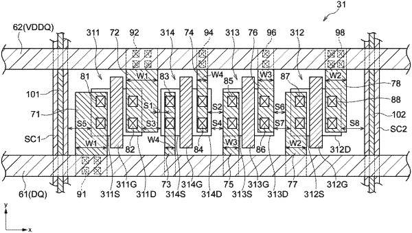
a main driver comprising a plurality of transistors including a first transistor and a second transistor connected in parallel;
wherein the first transistor comprises a first wiring pattern and a second wiring pattern and the second transistor comprises a third wiring pattern and a fourth wiring pattern,
wherein first and second wiring patterns of the first transistor have a greater width in a first direction than the third and fourth wiring patterns of the second transistor,
wherein gate electrodes of the plurality of transistors are configured to connect to a ground potential or a first enable signal based on a wiring of a respective metal option, and
wherein the first transistor of the plurality of transistors is configured to receive the first enable signal and the second transistor of the plurality of transistors is configured to receive the ground potential.
|