| CPC G11C 11/4091 (2013.01) [G11C 7/065 (2013.01); G11C 7/12 (2013.01); G11C 8/08 (2013.01); G11C 11/4085 (2013.01); G11C 11/4094 (2013.01); G11C 7/14 (2013.01); G11C 11/4099 (2013.01)] | 15 Claims |
|
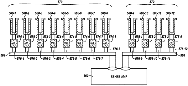
1. An apparatus, comprising:
a plurality of sense amplifiers, wherein each sense amplifier is coupled to a respective plurality of storage memory cells via a respective first digit line and a respective plurality of offset memory cells via a respective second digit line; and
a respective plurality of access devices coupled to the respective plurality of offset memory cells and the respective second digit line,
wherein respective voltages held capacitively by the plurality of storage memory cells correspond to data values, wherein respective voltages held capacitively by the plurality of offset memory cells do not correspond to data values, and wherein the plurality of offset memory cells have a cumulative capacitance that is approximately equal to a capacitance of the first digit line.
|