| CPC G09G 3/3674 (2013.01) [G11C 19/28 (2013.01); G09G 2310/0286 (2013.01); G09G 2330/06 (2013.01)] | 15 Claims |
|
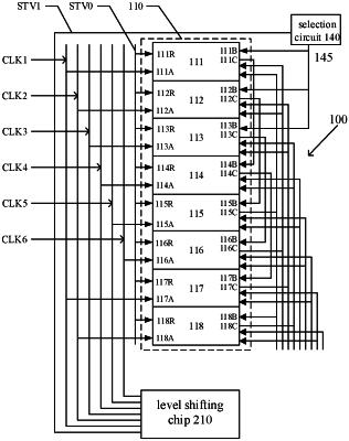
1. A gate driving circuit, comprising a plurality of shift register units as cascaded, wherein the plurality of shift register units as cascaded comprise:
a first shift register unit comprising a first clock signal terminal,
an (n+1)-th shift register unit comprising an (n+1)-th clock signal terminal,
a second shift register unit comprising a second clock signal terminal, and
an (n+2)-th shift register unit comprising an (n+2)-th clock signal terminal;
the gate driving circuit further comprises a first clock signal line connected to the first clock signal terminal and the (n+1)-th clock signal terminal, and a second clock signal line connected to the second clock signal terminal and the (n+2)-th clock signal terminal; and
the first clock signal line and the second clock signal line are arranged spaced apart, an input terminal of the first clock signal line is connected to one terminal of a first resistor, an input terminal of the second clock signal line is connected to one terminal of a second resistor, a resistance value of the second resistor is larger than a resistance value of the first resistor, and n is a positive integer greater than or equal to 2, n is a total number of clock signal lines.
|