| CPC G09G 3/2092 (2013.01) [G09G 2300/0426 (2013.01); G09G 2310/0286 (2013.01); G09G 2310/061 (2013.01)] | 20 Claims |
|
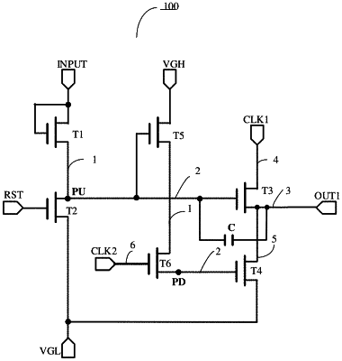
1. A shift register unit, comprising a substrate, an input circuit, a reset circuit, a first output circuit, a first output terminal, a first connection conductive portion connecting both the input circuit and the reset circuit, a second connection conductive portion connecting both the reset circuit and the first output circuit, a third connection conductive portion connecting both the first output circuit and the first output terminal, a first signal line input terminal, a fourth connection conductive portion, an output noise reduction circuit, a fifth connection conductive portion, a control circuit, a second signal line input terminal and a sixth connection conductive portion,
wherein the input circuit, the reset circuit, the first output circuit, the first output terminal, the first connection conductive portion, the second connection conductive portion, and the third connection conductive portion are all on the substrate, and
wherein the input circuit is configured to control a level of a first node in response to an input signal;
the reset circuit is configured to reset the first node in response to a reset signal;
the first output circuit is configured to output a first signal to the first output terminal under control of the level of the first node;
the fourth connection conductive portion connects the first output circuit and the first signal line input terminal;
the output noise reduction circuit is configured to perform noise reduction on the first output terminal under control of a level of a second node;
the fifth connection conductive portion connects the output noise reduction circuit and the first output circuit;
the control circuit is configured to control the level of the second node under control of the level of the first node and/or a second signal; and
the sixth connection conductive portion is configured to connect the control circuit and the second signal line input terminal, and
wherein a length of the first connection conductive portion is less than a length of the second connection conductive portion.
|