| CPC G09G 3/2092 (2013.01) [G09G 2310/0286 (2013.01); G09G 2310/061 (2013.01); G09G 2310/08 (2013.01)] | 17 Claims |
|
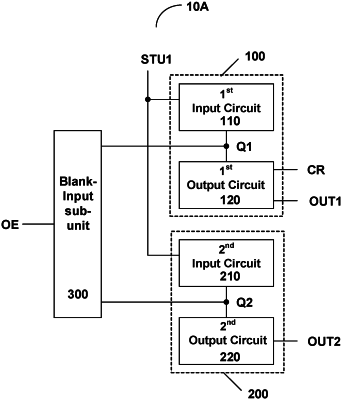
1. A shift-register unit, comprising:
a first circuit comprising a first input circuit coupled via a first node to a first output circuit, the first input circuit being configured to control a voltage level of the first node in response to a first input signal and the first output circuit being configured to output a shift-register signal and a first output signal in response to the voltage level of the first node;
a second circuit comprising a second input circuit coupled via a second node to a second output circuit, the second input circuit being configured to control a voltage level of the second node in response to the first input signal and the second output circuit being configured to output a second output signal in response to the voltage level of the second node; and
a blank-input circuit coupled to the first node and the second node, and being configured to receive a select-control signal to control respective voltage levels of the first node and the second node;
wherein the first input circuit and the second input circuit have a same circuit structure;
the first output signal and the second output signal are different from each other;
the blank-input circuit comprises a common-input circuit, a first transport circuit, and a second transport circuit;
the common-input circuit being configured to control a voltage level of a third node in response to the select-control signal and to control a voltage level of a fourth node;
the first transport circuit being coupled to the first node and the fourth node, and being configured to control the voltage level of the first node in response to the voltage level of the fourth node or a first transport signal; and
the second transport circuit being coupled to the second node and the fourth node, and being configured to control the voltage level of the second node in response to the voltage level of the fourth node or a second transport signal.
|