| CPC G06F 30/367 (2020.01) [G03F 1/36 (2013.01); G03F 1/78 (2013.01); G03F 1/80 (2013.01); G03F 1/86 (2013.01)] | 24 Claims |
|
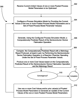
1. A computer-implemented method of optimizing a process simulation model that predicts a result of a semiconductor device fabrication operation from process parameter values characterizing the semiconductor device fabrication operation, the method comprising:
(a) providing, to a process simulation model, current values of one or more floated process model parameters to be optimized and a set of fixed process model parameter value(s);
(b) generating, using the process simulation model, a computationally predicted result of the semiconductor device fabrication operation, wherein the computationally predicted result comprises depth information of a substrate feature determined from the process simulation model;
(c) comparing the computationally predicted result of the semiconductor device fabrication operation with a metrology result obtained from one or more substrate features produced, at least in part, by performing the semiconductor device fabrication operation in a reaction chamber operating under the set of fixed process parameter values; and
(d) generating an update of the current values of the one or more floated process model parameters for use in the process simulation model based at least on a comparison of depth information associated with the computationally predicted result of the semiconductor device fabrication operation with depth information associated with the metrology result.
|