| CPC G06F 11/3037 (2013.01) [G06F 3/064 (2013.01); G06F 3/0619 (2013.01); G06F 3/0679 (2013.01); G06F 11/076 (2013.01); G06F 11/3058 (2013.01)] | 17 Claims |
|
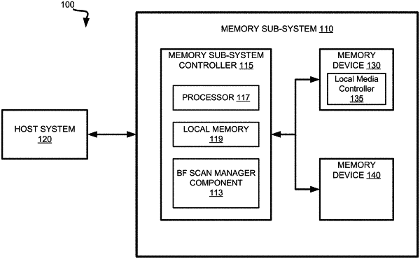
1. A system comprising:
a memory device; and
a processing device, operatively coupled to the memory device, to perform operations comprising:
identifying an operating temperature of the memory device;
identifying, for a set of blocks of the memory device, a scan frequency corresponding to the operating temperature, wherein the scan frequency exceeds one scan operation per a period of time in which the set of blocks stays associated with a certain threshold voltage offset;
responsive to determining that the operating temperature exceeds a threshold temperature, increasing the scan frequency; and
performing a scan operation with respect to a representative block of the set of blocks of the memory device at the scan frequency.
|