| CPC G06F 3/0659 (2013.01) [G06F 3/0604 (2013.01); G06F 3/0656 (2013.01); G06F 3/0679 (2013.01); G11C 16/0483 (2013.01); G11C 11/56 (2013.01)] | 39 Claims |
|
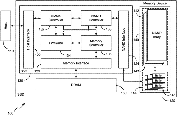
1. A memory storage system comprising:
a non-volatile semiconductor memory device comprising a memory array and a plurality of buffers; and
a controller in communication with the plurality of buffers, and configured to issue a first command to the non-volatile semiconductor memory device to cause a transfer of a data payload from the controller to a subset of n first buffers of the plurality of buffers, the data payload to be encoded by the non-volatile semiconductor memory device,
wherein the controller is further configured to issue a second command to the non-volatile semiconductor memory device to cause the data payload in the subset of n first buffers to be encoded in n second buffers of the plurality of buffers separate from the n first buffers, and stored in the memory array.
|