| CPC G06F 3/0412 (2013.01) [G06F 3/044 (2013.01); G06F 3/046 (2013.01); G06F 3/0418 (2013.01); G06F 3/0445 (2019.05); G06F 3/0446 (2019.05); G06F 3/04164 (2019.05); G06F 3/04166 (2019.05); G09G 3/344 (2013.01); G09G 3/3696 (2013.01); G06F 2203/04106 (2013.01); G06F 2203/04112 (2013.01); G09G 2300/0426 (2013.01); G09G 2310/0202 (2013.01); G09G 2310/068 (2013.01); G09G 2310/08 (2013.01)] | 17 Claims |
|
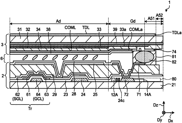
1. A display device comprising:
a substrate;
a plurality of first electrodes;
a plurality of pixel electrodes;
a display functional layer;
a common electrode opposed to the pixel electrodes;
a plurality of second electrodes;
a plurality of third electrodes; and
a controller configured to generate a plurality of display periods and a plurality of sensing periods in a time-division manner by controlling the first electrodes, the pixel electrodes, the common electrode, and the third electrodes,
wherein the substrate, the third electrodes, the pixel electrodes, the display functional layer, and the common electrode are stacked in the order as listed, a distance between the third electrode and the pixel electrode is less than a distance between the common electrode and the pixel electrode,
wherein the first electrodes and the second electrodes are provided in a same layer, and an insulating layer is provided between the common electrode and the first and second electrodes,
wherein, during the display periods, in response to a control signal from the controller, the pixel electrodes are supplied with a pixel signal through the lines, and the common electrode and the third electrodes are supplied with a common signal, and
wherein, during the sensing periods, in response to the control signal from the controller, the first electrodes are supplied with a drive signal to generate electrostatic capacitance between themselves and the second electrodes, synchronously or asynchronously with the display periods.
|