| CPC G02F 1/136213 (2013.01) [G02F 1/1368 (2013.01); G02F 1/136286 (2013.01)] | 9 Claims |
|
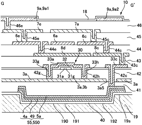
1. An electro-optical device comprising:
a substrate body provided with a groove;
an insulating film layered on the substrate body in a region including the groove; and
a layered film layered on the insulating film, wherein
the layered film is provided along a side surface and a bottom surface of the groove with the insulating film disposed therebetween,
an opening width of the groove is from 0.6 μm to 1.0 μm, and
a thickness of the insulating film is from 0.05 μm to 0.3 μm.
|