| CPC G02F 1/13338 (2013.01) [G02F 1/13318 (2013.01); G02F 1/13394 (2013.01); G02F 1/133512 (2013.01); G02F 1/134309 (2013.01); G06V 40/1318 (2022.01); G02F 1/133707 (2013.01)] | 9 Claims |
|
1. A display device comprising:
a first substrate;
a second substrate opposing the first substrate;
a liquid crystal layer arranged between the first substrate and the second substrate;
an optical sensor arranged between the first substrate and the liquid crystal layer;
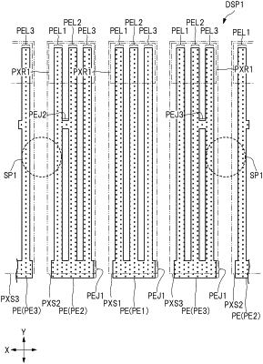
a plurality of pixels composed of a first sub-pixel, a second sub-pixel arranged next to one end of the first sub-substrate in a first direction, a third sub-pixel arranged next to the other end of the first sub-pixel in the first direction;
a plurality of pixel electrodes arranged between the liquid crystal layer and the first substrate;
a first light-shielding film formed between the liquid crystal layer and the second substrate and formed in a matrix so as to partition each of the first sub-pixel, the second sub-pixel, and the third sub-pixel; and
a first spacer member arranged between the first substrate and the second substrate and mainlining a thickness of the liquid crystal layer,
wherein each of the first sub-pixel, the second sub-pixel, and the third sub-pixel includes:
a visible light transmitting region that transmits visible light via a display opening formed in the first light-shielding film; and
a light-shielding region arranged next to the visible light transmitting region in a second direction intersecting with the first direction, and covered with the first light-shielding film,
each of the plurality of pixel electrodes includes:
a first line portion, a second line portion, and a third portion that extend in the second direction and are arranged so as to separate from one another at one end portions thereof; and
a first connecting portion formed so as to connect the respective other end portions of the first line portion, the second line portion, and the third line portion,
the plurality of pixel electrodes includes a first pixel electrode arranged on the first sub-pixel, a second pixel electrode arranged on the second sub-pixel, and a third pixel electrode arranged on the third sub-pixel,
the spacer member is arranged at a position overlapping with the first line portion of the second pixel electrode in a plan view,
the second pixel electrode further has a second connecting portion that connects the first line portion and a second line portion arranged next to the first line portion, and
the second connecting portion of the second pixel electrode is arranged between a region where the first line portion of the second pixel electrode overlaps with the first spacer member and the one end portion of the first line portion of the second pixel electrode.
|