| CPC G02B 26/0833 (2013.01) | 20 Claims |
|
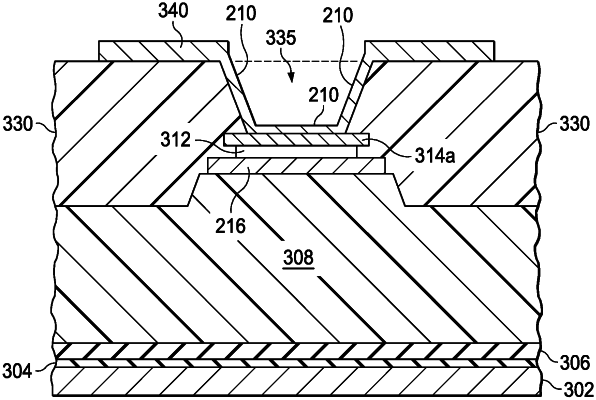
1. A method, comprising:
forming an aluminum silicon layer on a metal layer;
forming a titanium nitride layer on a surface of the aluminum silicon layer opposite the metal layer;
etching the titanium nitride layer to create a titanium nitride pad;
forming a torsion hinge in the metal layer, wherein the titanium nitride pad is on the torsion hinge;
depositing a sacrificial layer over the torsion hinge and titanium nitride pad;
forming a via in the sacrificial layer from a surface of the sacrificial layer opposite the torsion hinge to the titanium nitride pad;
depositing a metal mirror layer on a surface of the sacrificial layer opposite the torsion hinge and in the via on the titanium nitride pad; and
removing the sacrificial layer.
|