| CPC G01R 19/16519 (2013.01) [G01R 19/145 (2013.01); G01R 19/16552 (2013.01); G01R 31/40 (2013.01); G01R 31/52 (2020.01)] | 4 Claims |
|
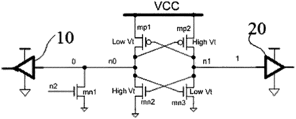
1. A power failure detection circuit, comprising a first PMOS FET (mp1), a second PMOS PET (mp2), a first NMOS FET (mn2), a second NMOS PET (mn3) and a reset transistor (mn1), wherein the source electrode of the first PMOS FET (mp1) is connected with a power supply terminal (VCC), the gate electrode of the first PMOS FET (mp1) is connected with the drain electrode of the second PMOS FET (mp2), and the drain electrode of the first PMOS FET (mp1) is connected with the drain electrode of the first NMOS PET (mn2); the source electrode of the second PMOS FET (mp2) is connected with the power supply terminal (VCC), the gate electrode of the second PMOS FET (mp2) is connected with the drain electrode of the first PMOS FET (mp1), and the drain electrode of the second PMOS FET (mp2) is connected with the drain electrode of the second NMOS FET (mn3); the gate electrode of the first NMOS FET (mn2) is connected with the drain electrode of the second NMOS FET (mn3); the source electrode of the first NMOS FET (mn2) is grounded; the gate electrode of the second NMOS FET (mn3) is connected with the drain electrode of the first NMOS PET (mn2), and the source electrode of the second NMOS FET (mn3) is grounded;
the PN junction area of the drain electrode of the first PMOS PET (mp1) is greater than the PN junction area of the drain electrode of the first NMOS FET (mn2); the PN junction area of the drain electrode of the second NMOS FET (mn3) is greater than the PN junction area of the drain electrode of the second PMOS FET (mp2); and a current electrode of the reset transistor (mn1) is electrically connected with the drain electrode of the first PMOS FET (mp1) to output a reset electrical signal.
|