| CPC G01N 33/551 (2013.01) [G01N 29/022 (2013.01); G01N 29/036 (2013.01); H01L 29/1606 (2013.01)] | 6 Claims |
|
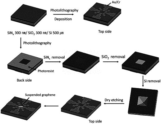
1. A fabrication method for a biosensor, comprising:
applying a photoresist on an insulating substrate;
exposing a first surface of the insulating substrate, etching the photoresist, and then forming an electrode;
forming a pattern for manufacturing a membrane on a second surface of the insulating substrate;
forming the membrane on the first surface by an etching process and solvent treatment on the second surface of the insulating substrate;
removing the formed membrane;
stacking a graphene-polymer layer on a hollow structure formed at a portion from which the membrane of the first surface is removed, wherein the graphene-polymer layer is exactly placed on the hollow structure while checking the location of the graphene-polymer layer relative to the hollow structure;
curing the graphene in the graphene-polymer layer by heat treatment of the graphene at 30-70° C. to fix the graphene on the hollow structure;
further heat treating the graphene-polymer layer to at least 180° C. to remove the polymer from the graphene-polymer layer, thereby leaving a cured graphene layer;
subjecting the cured graphene to oxygen plasma treatment to further fix and immobilize the cured graphene layer on the hollow structure without gaps;
forming a resonance unit by treating a surface exposed to an outside of the graphene layer with a surface treatment agent containing a functional group; and
coupling a detection unit to the resonance unit including the functional group, and
wherein the insulating substrate has a SiO2 layer and a SiNx layer which are sequentially stacked on both surfaces of the insulating substrate, and x is a real number between 1 and 5, and
wherein an inner area of the hollow structure is 6.0×102 μm2 to 6.3×102 μm2.
|