US 11,702,760 B2
N-type silicon single crystal production method, n-type silicon single crystal ingot, silicon wafer, and epitaxial silicon wafer
Koichi Maegawa, Tokyo (JP); Yasuhito Narushima, Tokyo (JP); Yasufumi Kawakami, Tokyo (JP); Fukuo Ogawa, Tokyo (JP); and Ayumi Kihara, Tokyo (JP)
Assigned to SUMCO CORPORATION, Tokyo (JP)
Appl. No. 16/605,320
Filed by SUMCO CORPORATION, Tokyo (JP)
PCT Filed Mar. 20, 2018, PCT No. PCT/JP2018/011125
§ 371(c)(1), (2) Date Oct. 15, 2019,
PCT Pub. No. WO2018/198606, PCT Pub. Date Nov. 1, 2018.
Claims priority of application No. JP2017-086530 (JP), filed on Apr. 25, 2017; and application No. JP2017-086532 (JP), filed on Apr. 25, 2017.
Prior Publication US 2020/0141024 A1, May 7, 2020
This patent is subject to a terminal disclaimer.
Int. Cl. C30B 15/04 (2006.01); C30B 15/10 (2006.01); C30B 29/06 (2006.01); C30B 35/00 (2006.01); H01L 21/02 (2006.01)
CPC C30B 15/04 (2013.01) [C30B 15/10 (2013.01); C30B 29/06 (2013.01); C30B 35/002 (2013.01); C30B 35/007 (2013.01); H01L 21/02002 (2013.01)] 3 Claims
OG exemplary drawing
 
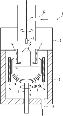
1. A producing method of an n-type monocrystalline silicon by pulling up the n-type monocrystalline silicon from a silicon melt comprising a main dopant in a form of red phosphorus and growing the n-type monocrystalline silicon according to a Czochralski process,
wherein:
the n-type monocrystalline silicon comprises a straight-body diameter ranging from 301 mm to 330 mm, and
the n-type monocrystalline silicon, a part of which exhibits an electrical resistivity ranging from 0.8 mΩcm to 1.0 mΩcm, is pulled up using a quartz crucible whose inner diameter ranges from 1.7-fold to 2.0-fold relative to a straight-body diameter of the n-type monocrystalline silicon.