| CPC C23C 16/4585 (2013.01) [C23C 16/4581 (2013.01); C23C 16/4586 (2013.01); C23C 16/505 (2013.01); H01L 21/68742 (2013.01); H01L 21/68757 (2013.01); H01L 21/68785 (2013.01)] | 8 Claims |

|
1. An assembly for use in a process chamber, comprising:
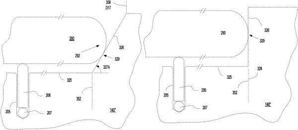
a pedestal having a pedestal top surface extending from a central axis of the pedestal, the pedestal top surface having a plurality of wafer supports configured to support a wafer at a wafer support level above the pedestal top surface, wherein the pedestal top surface is horizontally oriented along a first plane perpendicular to the central axis;
a raised annular rim configured on an outer region of the pedestal top surface and configured to block lateral movement of the wafer that is resting on the pedestal, the raised annular rim having a mesa surface rising above the pedestal top surface, the raised annular rim and pedestal top surface forming a pocket configured to receive the wafer, wherein the mesa surface is horizontally oriented along a second plane perpendicular to the central axis, wherein the first plane and the second plane are in parallel; and
a beveled surface extending from an inner diameter of the raised annular rim to an outer diameter of the pocket on the pedestal top surface and configured to support a wafer, wherein the beveled surface rises uniformly from the pedestal top surface to the mesa surface of the raised annular rim at an angle taken with respect to the pedestal top surface that is less than 90 degrees, wherein each of the plurality of wafer supports sits within a hole that opens up at the pedestal top surface and rests on a compliant spacer that sits at a bottom of the hole, wherein the compliant spacer is configured to prevent each of the wafer supports from breaking and/or for height modulation;
a recess in the pedestal top surface centered about the central axis, the recess having a recess top surface; and
a lift pad configured to support the wafer,
wherein the recess is configured to receive the lift pad when the lift pad is resting on the recess top surface,
wherein a pad top surface of the lift pad is coplanar with the pedestal top surface when the lift pad is resting on the recess top surface,
wherein a coplanar surface including the pedestal top surface and the pad top surface when the lift pad is resting on the recess top surface is flat,
wherein the mesa surface extends from the outer diameter of the pocket to a curved surface that joins the mesa surface to the outer edge of the pedestal, wherein the outer edge of the pedestal is vertically oriented relative to the mesa surface.
|