US 11,702,733 B2
Methods for depositing blocking layers on conductive surfaces
Lakmal C. Kalutarage, San Jose, CA (US); Bhaskar Jyoti Bhuyan, San Jose, CA (US); Aaron Dangerfield, San Jose, CA (US); Feng Q. Liu, San Jose, CA (US); Mark Saly, Santa Clara, CA (US); Michael Haverty, Mountain View, CA (US); and Muthukumar Kaliappan, Fremont, CA (US)
Assigned to Applied Materials, Inc., Santa Clara, CA (US)
Filed by Applied Materials, Inc., Santa Clara, CA (US)
Filed on May 7, 2021, as Appl. No. 17/315,223.
Prior Publication US 2022/0372616 A1, Nov. 24, 2022
Int. Cl. C23C 16/04 (2006.01); C23C 16/02 (2006.01); H01L 21/02 (2006.01); H01L 21/32 (2006.01); C23C 16/56 (2006.01)
CPC C23C 16/042 (2013.01) [C23C 16/0272 (2013.01); C23C 16/56 (2013.01); H01L 21/0228 (2013.01); H01L 21/02172 (2013.01); H01L 21/32 (2013.01); H01L 21/0217 (2013.01); H01L 21/02211 (2013.01)] 13 Claims
OG exemplary drawing
 
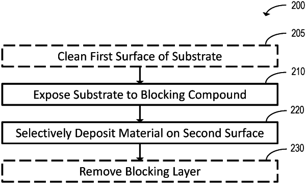
1. A method of selectively depositing a blocking layer, the method comprising exposing a substrate comprising a metallic material having a first surface and a dielectric material having a second surface to a blocking compound to selectively form a blocking layer on the first surface over the second surface, the blocking compound comprising a 4-8 member heterocyclic ring comprising at least one heteroatom and at least one substituent group selected from alkyl or aryl groups comprising 1-8 carbon atoms, wherein the heterocyclic ring is a 2-aminomethyl heterocycle.