| CPC H10N 70/883 (2023.02) [G11C 13/0007 (2013.01); H10B 63/00 (2023.02); H10N 70/021 (2023.02); H10N 70/841 (2023.02)] | 20 Claims |
|
1. A method comprising:
depositing a bottom electrode layer over a substrate;
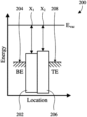
depositing a dielectric film over and directly on the bottom electrode layer, wherein the dielectric film comprises multiple different dielectric layers that are vertically stacked, wherein the multiple different dielectric layers comprise a first dielectric layer at the bottom electrode layer, and wherein the first dielectric layer has a highest electron affinity amongst the multiple different dielectric layers;
depositing a top electrode layer over the dielectric film; and
patterning the bottom electrode layer, the dielectric film, and the top electrode layer into a memory cell;
wherein the multiple different dielectric layers further comprise a second dielectric layer, wherein the first dielectric layer comprises a first chemical compound with a first number of atoms of a metal element and a second number of atoms of a non-metal element, wherein the second dielectric layer comprises a second chemical compound with a third number of atoms of the metal element and a fourth number of atoms of the non-metal element, and wherein the first and third numbers are different and the second and fourth numbers are different.
|