US 11,696,486 B2
Mask, method for manufacturing the same, and method for manufacturing display panel
Jinoh Kwag, Yongin-si (KR); Sungsoon Im, Suwon-si (KR); Youngmin Moon, Yongin-si (KR); Ji-Hee Son, Hwaseong-si (KR); Seungyong Song, Suwon-si (KR); DuckJung Lee, Hwaseong-si (KR); and Hye Yong Chu, Hwaseong-si (KR)
Assigned to Samsung Display Co., Ltd., Yongin-si (KR)
Filed by Samsung Display Co., LTD., Yongin-si (KR)
Filed on Oct. 11, 2020, as Appl. No. 17/67,730.
Claims priority of application No. 10-2020-0004066 (KR), filed on Jan. 13, 2020.
Prior Publication US 2021/0217997 A1, Jul. 15, 2021
Int. Cl. H01L 51/56 (2006.01); C23C 14/04 (2006.01); H01L 51/00 (2006.01); H01L 27/32 (2006.01); H10K 71/00 (2023.01); H10K 59/121 (2023.01); H10K 71/16 (2023.01)
CPC H10K 71/00 (2023.02) [C23C 14/042 (2013.01); H10K 59/121 (2023.02); H10K 71/166 (2023.02)] 16 Claims
OG exemplary drawing
 
1. A mask having a plurality of cell areas, each of which has a plurality of through-portions defined therein,
the mask comprising:
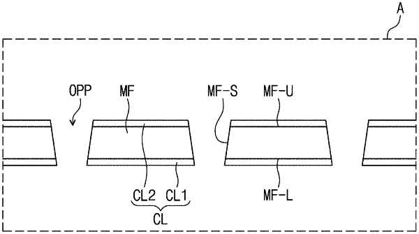
a mask film comprising a polymer; and
a conductive layer disposed on at least one surface of the mask film and comprising conductive metal or a conductive metal oxide,
wherein the conductive layer covers each of a top surface and a bottom surface of the mask film.