| CPC H10K 59/40 (2023.02) [G06F 3/0446 (2019.05); H10K 50/844 (2023.02); H10K 59/122 (2023.02); H10K 59/131 (2023.02); H10K 77/111 (2023.02); G06F 2203/04111 (2013.01)] | 20 Claims |
|
1. A display panel, comprising:
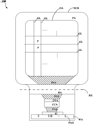
a substrate, a display area, a peripheral area and a welding area, wherein the peripheral area surrounds the display area, and the welding area is positioned on a side of the peripheral area away from the display area;
at least one barrier disposed on the substrate, the barrier being located in the peripheral area and surrounding the display area, the barrier comprising a single-sided barrier structure located between the display area and the welding area;
an organic insulating structure disposed on the substrate, the organic insulating structure comprising a plurality of sub-insulating structures disposed in a stacked manner, a portion of each of the sub-insulating structures being located in the display area, each of the sub-insulating structures having a first boundary located between the display area and the single-sided barrier structure, wherein, for any adjacent two of the sub-insulating structures, the first boundary of the sub-insulating structure on a side away from the substrate is closer to the display area than the first boundary of the sub-insulating structure on a side proximal to the substrate; a distance between first boundaries of any adjacent two of the sub-insulating structures is greater than or equal to 20 μm;
a touch electrode pattern arranged on a side of the organic insulating structure away from the substrate;
a touch signal line arranged on a side of the organic insulating structure away from the substrate, a terminal of the touch signal line is electrically coupled to the touch electrode pattern, another terminal of the touch signal line is coupled to the welding area, and an orthographic projection of a portion, in the peripheral area, of the touch signal line on the substrate intersects with the first boundary of each of the sub-insulating structures.
|