US 11,696,478 B2
Display panel for improving display effect in low-resolution area, manufacturing method thereof, and display device
Linhong Han, Beijing (CN); Yi Zhang, Beijing (CN); Hengzhen Liang, Beijing (CN); and Shikai Qin, Beijing (CN)
Assigned to Chengdu BOE Optoelectronics Technology Co., Ltd., Sichuan (CN); and BOE Technology Group Co., Ltd., Beijing (CN)
Filed by CHENGDU BOE OPTOELECTRONICS TECHNOLOGY CO., LTD., Sichuan (CN); and BOE TECHNOLOGY GROUP CO., LTD., Beijing (CN)
Filed on Nov. 29, 2021, as Appl. No. 17/536,868.
Application 17/536,868 is a continuation of application No. 16/623,180, granted, now 11,211,430, previously published as PCT/CN2019/073476, filed on Jan. 28, 2019.
Prior Publication US 2022/0085118 A1, Mar. 17, 2022
This patent is subject to a terminal disclaimer.
Int. Cl. H10K 59/35 (2023.01); H10K 59/60 (2023.01); H10K 59/122 (2023.01); H10K 71/00 (2023.01); H10K 71/16 (2023.01); H10K 59/12 (2023.01)
CPC H10K 59/352 (2023.02) [H10K 59/122 (2023.02); H10K 59/351 (2023.02); H10K 59/60 (2023.02); H10K 71/00 (2023.02); H10K 71/164 (2023.02); H10K 71/166 (2023.02); H10K 59/1201 (2023.02)] 16 Claims
OG exemplary drawing
 
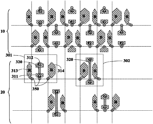
1. A display panel, comprising:
a first area and a second area, a pixel density of the first area being greater than a pixel density of the second area;
wherein the second area comprises at least a first sub-pixel and a second sub-pixel, the first sub-pixel and the second sub-pixel share one sub-pixel driving circuit, and emission color of the first sub-pixel is the same as emission color of the second sub-pixel.